Open Source Hardware

FOC BLDC Motor Controller

A high-performance Field-Oriented Control driver built around the STM32G474 MCU and DRV8308 gate driver. Designed for precision robotics, drones, and automation.

32V Max Voltage
170MHz STM32G474
6x MOSFETs
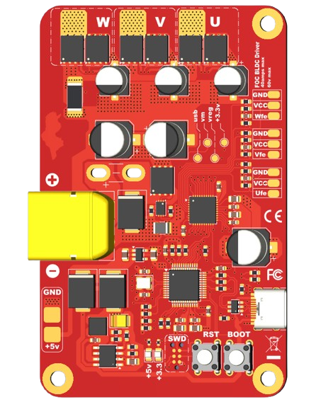
FOC BLDC Driver PCB 3D Render
DRV8308
STM32G474
USB-C

Built for Performance

Everything you need for precise motor control in a compact, single-board design.

◈

STM32G474 MCU

ARM Cortex-M4 at 170 MHz with hardware FPU, CORDIC, and FMAC accelerators for real-time FOC computation.

⚡

DRV8308 Gate Driver

Integrated 3-phase predriver with configurable 10-130 mA gate drive, Hall commutation, and SPI configuration.

◎

Field-Oriented Control

Sinusoidal PWM and Space Vector modulation for smooth, efficient torque control with minimal audible noise.

◉

Hall Sensor Inputs

Three independent Hall sensor channels with 4.7kΩ pull-ups and VREG-powered supply for reliable commutation.

🛡

Full Protection

Reverse polarity, overcurrent, undervoltage, and overtemperature protection with fault reporting via FAULTn pin.

🔌

USB-C & SWD

USB Type-C for power and data, plus ARM SWD debug header for firmware development and real-time debugging.

Board Architecture

Understanding the circuit blocks and signal flow of the FOC driver.

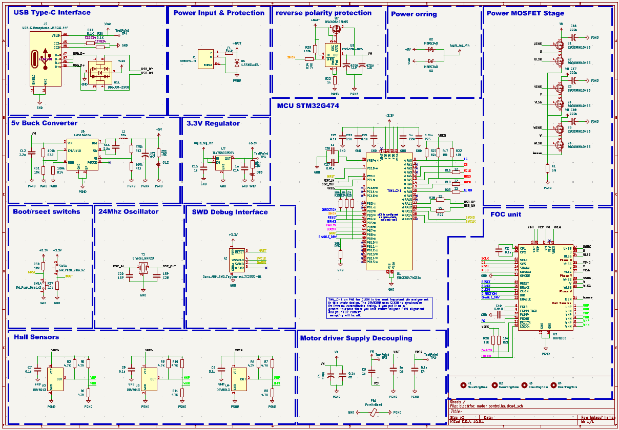
Full Schematic

Power Input & Protection

  • XT60PW-M connector for +BATT (8.5V-32V)
  • Fuse F1 with reverse polarity diode D1
  • LTC4359 ideal diode for reverse polarity protection
  • Power ORing with MBRS340 Schottky diodes

MCU - STM32G474CBTx

  • 170 MHz Cortex-M4 with FPU
  • TIM1_CH1 on PA8 for DRV8308 CLKIN
  • SPI1 on PA4-PA7 for DRV config
  • USB_DP/DN on PA11-PA12
  • SWD on PA13-PA14

DRV8308 FOC Unit

  • 3-phase N-channel MOSFET predriver
  • 10-130 mA configurable gate drive
  • Hall sensor inputs (UHP/UHN, VHP/VHN, WHP/WHN)
  • Current sense via ISEN (5mOhm shunt R1)
  • SPI configuration & fault reporting

Power Stage

  • 6x BSC098N10NS5 MOSFETs (100V, 9.8mOhm)
  • 3-phase bridge: U, V, W outputs
  • 220uF bulk capacitors per phase
  • PGND star grounding

Regulators

  • LM5164DDA 5V buck converter (VM -> +5V)
  • TLV75533 3.3V LDO (+5V -> +3.3V)
  • VREG from DRV8308 for Hall sensors
  • Decoupling: 470uF + 0.1uF per rail

Peripherals

  • USB Type-C with ESD protection (USBLC6-2SC6)
  • 24 MHz crystal oscillator (Y1)
  • BOOT & RESET tactile switches
  • 3x DRV5013 Hall sensors (U3, U4, U5)

Power Tree

The board accepts 8.5V-32V via the XT60PW-M connector (J1). A fuse (F1) and reverse-polarity diode (D1, 1.55MCxxCA) protect against wiring mistakes. The LTC4359 (U8) acts as an ideal diode controller for the main power path. The LM5164DDA (U6) buck converter steps VM down to +5V, which feeds the TLV75533 (U7) LDO for clean +3.3V logic supply. The DRV8308 generates its own VREG (typically 5V) to power external Hall sensors.

Input Voltage8.5V - 32V DC
5V BuckLM5164DDA, up to 1A
3.3V LDOTLV75533PDBV, 500mA
VREG (Hall)DRV8308 internal, ~5V
Reverse PolarityLTC4359 + MBRS340

STM32G474 Pin Assignment

The STM32G474CBTx is the brain of the driver. TIM1_CH1 on PA8 is the most critical pin - it provides the CLKIN signal to the DRV8308, synchronizing internal commutation timing. If moved to a general-purpose timer, center-aligned PWM alignment and FOC current sampling will be off. The MCU communicates with DRV8308 via SPI1 (PA4=CS, PA5=SCLK, PA6=MISO, PA7=MOSI).

Pin Function Type Connected To
PA8TIM1_CH1 / CLKINPWMDRV8308 CLKIN
PA4SPI1_NSS / CSSPIDRV8308 SCS
PA5SPI1_SCK / SCLKSPIDRV8308 SCLK
PA6SPI1_MISO / SDATAOSPIDRV8308 SDATAO
PA7SPI1_MOSI / SDATAISPIDRV8308 SDATAI
PB0DIRECTIONCTRLDRV8308 DIR
PB1SHDNCTRLDRV8308 SHDN
PB2RESETCTRLDRV8308 RESET
PB3BRAKECTRLDRV8308 BRAKE
PB4FAULTnCTRLDRV8308 FAULTn
PB5LOCKnCTRLDRV8308 LOCKn
PB6FGINN / FGOUTCTRLDRV8308 FGOUT
PB7ENABLE_DRVCTRLDRV8308 ENABLE
PA11USB_DMUSBUSB-C D-
PA12USB_DPUSBUSB-C D+
PA13SWDIODEBUGSWD Header
PA14SWCLKDEBUGSWD Header

DRV8308 Operation Modes

The DRV8308 supports three speed input modes: Clock Frequency (closed-loop RPM matching), Clock Duty Cycle (open-loop PWM), and Register Speed (SPI duty cycle). In Clock Frequency mode, the DRV8308 uses Hall sensors or FG trace to measure motor speed and matches it to the CLKIN reference. The device transitions to single-Hall operation after lock-up to minimize jitter, and can drive sinusoidal (180 degree) currents for quiet FOC operation.

Gate Drive

  • High-side: VM + 10V (VCP charge pump)
  • Low-side: 10V (VM referenced)
  • Configurable IDRIVE: 10-130 mA
  • Dead-time & synchronous rectification

Protection Features

  • Cycle-by-cycle current limit (0.25V across R1)
  • Overvoltage & undervoltage lockout
  • Overtemperature shutdown
  • Rotor lock detection
  • FAULTn open-drain output

Getting Started

Example firmware for STM32 HAL and Arduino (SimpleFOC) to spin your motor.

main.c - STM32G474 FOC Initialization
/* FOC BLDC Motor Driver - STM32G474 HAL Example
 * Hardware: STM32G474CBTx + DRV8308
 * TIM1_CH1 (PA8) -> DRV8308 CLKIN (critical!)
 * SPI1 (PA4-PA7) -> DRV8308 config
 */

#include "main.h"

/* DRV8308 Register Addresses */
#define DRV8308_FAULT1      0x00
#define DRV8308_FAULT2      0x01
#define DRV8308_SYSOPT1     0x02
#define DRV8308_SYSOPT2     0x03
#define DRV8308_SYSOPT3     0x04
#define DRV8308_SYSOPT4     0x05
#define DRV8308_SYSOPT5     0x06
#define DRV8308_SYSOPT6     0x07
#define DRV8308_SYSOPT7     0x08
#define DRV8308_SYSOPT8     0x09
#define DRV8308_SYSOPT9     0x0A

SPI_HandleTypeDef hspi1;
TIM_HandleTypeDef htim1;

/* DRV8308 SPI Write */
void DRV8308_WriteReg(uint8_t addr, uint16_t data) {
    uint8_t tx[3];
    tx[0] = (addr & 0x7F);          // Write command + address
    tx[1] = (data >> 8) & 0xFF;     // MSB
    tx[2] = data & 0xFF;            // LSB
    HAL_GPIO_WritePin(GPIOA, GPIO_PIN_4, GPIO_PIN_RESET); // CS low
    HAL_SPI_Transmit(&hspi1, tx, 3, 100);
    HAL_GPIO_WritePin(GPIOA, GPIO_PIN_4, GPIO_PIN_SET);   // CS high
}

/* DRV8308 SPI Read */
uint16_t DRV8308_ReadReg(uint8_t addr) {
    uint8_t tx[3] = {(addr | 0x80), 0x00, 0x00};
    uint8_t rx[3] = {0};
    HAL_GPIO_WritePin(GPIOA, GPIO_PIN_4, GPIO_PIN_RESET);
    HAL_SPI_TransmitReceive(&hspi1, tx, rx, 3, 100);
    HAL_GPIO_WritePin(GPIOA, GPIO_PIN_4, GPIO_PIN_SET);
    return ((rx[1] << 8) | rx[2]);
}

/* Initialize DRV8308 for FOC Sine Mode */
void DRV8308_Init(void) {
    // Release RESET
    HAL_GPIO_WritePin(GPIOB, GPIO_PIN_2, GPIO_PIN_SET);
    HAL_Delay(10);

    // SYSOPT1: Enable 180 degree sinusoidal commutation, set ENPOL
    // Bit 15: SINMODE=1 (180 degree sine), Bit 14: ENPOL=0 (active high)
    DRV8308_WriteReg(DRV8308_SYSOPT1, 0x8000);

    // SYSOPT2: Configure IDRIVE (gate drive current)
    // IDRIVE = 011 (50mA) for BSC098N10NS5
    DRV8308_WriteReg(DRV8308_SYSOPT2, 0x0300);

    // SYSOPT3: Dead time = 1us, PWM frequency aligned with TIM1
    DRV8308_WriteReg(DRV8308_SYSOPT3, 0x0040);

    // SYSOPT4: Advance angle = 0 degree, auto advance disabled
    DRV8308_WriteReg(DRV8308_SYSOPT4, 0x0000);

    // SYSOPT5: Speed loop proportional gain
    DRV8308_WriteReg(DRV8308_SYSOPT5, 0x1000);

    // SYSOPT6: Speed loop integral gain
    DRV8308_WriteReg(DRV8308_SYSOPT6, 0x0800);

    // SYSOPT7: FG filter & lock detection
    DRV8308_WriteReg(DRV8308_SYSOPT7, 0x0200);

    // SYSOPT8: Current limit blanking & deglitch
    DRV8308_WriteReg(DRV8308_SYSOPT8, 0x0000);

    // SYSOPT9: Overcurrent threshold (0.25V / R1 = 0.25V / 5mOhm = 50A)
    DRV8308_WriteReg(DRV8308_SYSOPT9, 0x0000);
}

/* TIM1 PWM for CLKIN (center-aligned, 20kHz) */
void TIM1_PWM_Init(void) {
    __HAL_RCC_TIM1_CLK_ENABLE();
    __HAL_RCC_GPIOA_CLK_ENABLE();

    GPIO_InitTypeDef GPIO_InitStruct = {0};
    GPIO_InitStruct.Pin = GPIO_PIN_8;
    GPIO_InitStruct.Mode = GPIO_MODE_AF_PP;
    GPIO_InitStruct.Pull = GPIO_NOPULL;
    GPIO_InitStruct.Speed = GPIO_SPEED_FREQ_HIGH;
    GPIO_InitStruct.Alternate = GPIO_AF6_TIM1;
    HAL_GPIO_Init(GPIOA, &GPIO_InitStruct);

    TIM_ClockConfigTypeDef sClockSourceConfig = {0};
    TIM_MasterConfigTypeDef sMasterConfig = {0};
    TIM_OC_InitTypeDef sConfigOC = {0};
    TIM_BreakDeadTimeConfigTypeDef sBreakDeadTimeConfig = {0};

    htim1.Instance = TIM1;
    htim1.Init.Prescaler = 0;
    htim1.Init.CounterMode = TIM_COUNTERMODE_CENTERALIGNED1;
    htim1.Init.Period = 4250;  // 170MHz / (2*4250) = 20kHz center-aligned
    htim1.Init.ClockDivision = TIM_CLOCKDIVISION_DIV1;
    htim1.Init.RepetitionCounter = 0;
    htim1.Init.AutoReloadPreload = TIM_AUTORELOAD_PRELOAD_ENABLE;
    HAL_TIM_PWM_Init(&htim1);

    sClockSourceConfig.ClockSource = TIM_CLOCKSOURCE_INTERNAL;
    HAL_TIM_ConfigClockSource(&htim1, &sClockSourceConfig);
    HAL_TIM_PWM_ConfigChannel(&htim1, &sConfigOC, TIM_CHANNEL_1);

    sConfigOC.OCMode = TIM_OCMODE_PWM1;
    sConfigOC.Pulse = 2125;  // 50% duty
    sConfigOC.OCPolarity = TIM_OCPOLARITY_HIGH;
    sConfigOC.OCNPolarity = TIM_OCNPOLARITY_HIGH;
    sConfigOC.OCFastMode = TIM_OCFAST_DISABLE;
    sConfigOC.OCIdleState = TIM_OCIDLESTATE_RESET;
    sConfigOC.OCNIdleState = TIM_OCNIDLESTATE_RESET;
    HAL_TIM_PWM_ConfigChannel(&htim1, &sConfigOC, TIM_CHANNEL_1);

    sBreakDeadTimeConfig.OffStateRunMode = TIM_OSSR_DISABLE;
    sBreakDeadTimeConfig.OffStateIDLEMode = TIM_OSSI_DISABLE;
    sBreakDeadTimeConfig.LockLevel = TIM_LOCKLEVEL_OFF;
    sBreakDeadTimeConfig.DeadTime = 0;
    sBreakDeadTimeConfig.BreakState = TIM_BREAK_DISABLE;
    sBreakDeadTimeConfig.BreakPolarity = TIM_BREAKPOLARITY_HIGH;
    sBreakDeadTimeConfig.AutomaticOutput = TIM_AUTOMATICOUTPUT_DISABLE;
    HAL_TIMEx_ConfigBreakDeadTime(&htim1, &sBreakDeadTimeConfig);

    HAL_TIM_PWM_Start(&htim1, TIM_CHANNEL_1);
}

/* Set motor speed via CLKIN frequency */
void Motor_SetSpeed(uint16_t freq_hz) {
    // DRV8308 matches motor RPM to CLKIN frequency
    // For 8-pole motor: RPM = freq_hz * 60 / 4 (pole pairs)
    // Update TIM1 ARR to change frequency while keeping 50% duty
    uint32_t arr = 170000000 / (2 * freq_hz);
    __HAL_TIM_SET_AUTORELOAD(&htim1, arr);
    __HAL_TIM_SET_COMPARE(&htim1, TIM_CHANNEL_1, arr / 2);
}

int main(void) {
    HAL_Init();
    SystemClock_Config();

    // Initialize SPI1, GPIOs, TIM1
    MX_SPI1_Init();
    MX_GPIO_Init();
    TIM1_PWM_Init();

    // Configure DRV8308
    DRV8308_Init();

    // Enable driver
    HAL_GPIO_WritePin(GPIOB, GPIO_PIN_7, GPIO_PIN_SET);   // ENABLE
    HAL_GPIO_WritePin(GPIOB, GPIO_PIN_1, GPIO_PIN_SET);   // SHDN release

    HAL_Delay(100);

    // Set direction
    HAL_GPIO_WritePin(GPIOB, GPIO_PIN_0, GPIO_PIN_SET);   // DIR = CW

    // Start motor at 500 Hz (approx 7500 RPM for 8-pole)
    Motor_SetSpeed(500);

    while (1) {
        // Monitor faults
        if (HAL_GPIO_ReadPin(GPIOB, GPIO_PIN_4) == GPIO_PIN_RESET) {
            uint16_t fault1 = DRV8308_ReadReg(DRV8308_FAULT1);
            uint16_t fault2 = DRV8308_ReadReg(DRV8308_FAULT2);
            // Handle fault...
        }
        HAL_Delay(10);
    }
}
foc_driver.ino - SimpleFOC Example
/**
 * FOC BLDC Driver - SimpleFOC Example
 * Compatible with STM32G474 (Arduino framework) + DRV8308
 * 
 * Connections:
 * - Motor phases U, V, W -> PCB outputs
 * - Hall sensors -> UHP/UHN, VHP/VHN, WHP/WHN
 * - Power: 12-24V to XT60
 * - USB-C for Serial & power
 */

#include <SimpleFOC.h>

// Hall sensor instance (3 sensors, 11 pole pairs example)
HallSensor sensor = HallSensor(2, 3, 4, 11);  // U, V, W pins

// Interrupt callbacks
void doA(){sensor.handleA();}
void doB(){sensor.handleB();}
void doC(){sensor.handleC();}

// BLDC motor & driver
BLDCMotor motor = BLDCMotor(11);  // 11 pole pairs (adjust!)
BLDCDriver3PWM driver = BLDCDriver3PWM(9, 10, 11, 8);  // PWM pins + enable

// Commander for serial control
Commander command = Commander(Serial);
void doTarget(char* cmd){ command.scalar(&target_velocity, cmd); }

float target_velocity = 0;

void setup() {
    Serial.begin(115200);
    delay(2000);
    Serial.println("FOC BLDC Driver initializing...");

    // Initialize Hall sensor
    sensor.init();
    sensor.enableInterrupts(doA, doB, doC);
    motor.linkSensor(&sensor);

    // Driver config
    driver.voltage_power_supply = 24;  // Your supply voltage
    driver.init();
    motor.linkDriver(&driver);

    // FOC modulation: Space Vector PWM for best efficiency
    motor.foc_modulation = FOCModulationType::SpaceVectorPWM;

    // Torque control mode (voltage-based)
    motor.torque_controller = TorqueControlType::voltage;
    motor.controller = MotionControlType::velocity;

    // Velocity PID tuning
    motor.PID_velocity.P = 0.2f;
    motor.PID_velocity.I = 0.1f;
    motor.PID_velocity.D = 0.0f;
    motor.PID_velocity.output_ramp = 1000;

    // Velocity low-pass filter
    motor.LPF_velocity.Tf = 0.01f;

    // Voltage limits
    motor.voltage_limit = driver.voltage_power_supply / 2;
    motor.velocity_limit = 50;  // rad/s

    // Current sense (if using DRV8308 ISEN)
    // InlineCurrentSense current_sense = InlineCurrentSense(0.005, 10, A0, A1, A2);
    // current_sense.init();
    // motor.linkCurrentSense(¤t_sense);

    // Initialize motor
    motor.init();

    // Align sensor and start FOC
    // For Hall sensors, this finds zero electrical angle
    motor.initFOC();

    // Add serial command
    command.add('T', doTarget, "target velocity");

    Serial.println("Motor ready! Send T to control.");
    Serial.println("Example: T20  (20 rad/s)");
}

void loop() {
    // Main FOC algorithm
    motor.loopFOC();

    // Motion control
    motor.move(target_velocity);

    // Serial user interface
    command.run();

    // Optional monitoring
    static unsigned long lastPrint = 0;
    if (millis() - lastPrint > 100) {
        lastPrint = millis();
        Serial.print("Vel: ");
        Serial.print(motor.shaft_velocity);
        Serial.print(" rad/s | Target: ");
        Serial.print(target_velocity);
        Serial.println();
    }
}
drv8308_regs.h - Register Map
/* DRV8308 Register Definitions
 * 16-bit registers, MSB first
 * Write:  addr[6:0] = 0, read addr[6:0] = 1
 */

#ifndef DRV8308_REGS_H
#define DRV8308_REGS_H

/* Fault Registers (Read-Only) */
#define REG_FAULT1      0x00
#define REG_FAULT2      0x01

/* System Option Registers (R/W) */
#define REG_SYSOPT1     0x02
#define REG_SYSOPT2     0x03
#define REG_SYSOPT3     0x04
#define REG_SYSOPT4     0x05
#define REG_SYSOPT5     0x06
#define REG_SYSOPT6     0x07
#define REG_SYSOPT7     0x08
#define REG_SYSOPT8     0x09
#define REG_SYSOPT9     0x0A

/* SYSOPT1 Bits */
#define SINMODE         (1 << 15)   // 1 = 180 degree sinusoidal, 0 = trapezoidal
#define ENPOL           (1 << 14)   // Enable polarity
#define DIRPOL          (1 << 13)   // Direction polarity
#define BRKPOL          (1 << 12)   // Brake polarity
#define SYNRECT         (1 << 11)   // Synchronous rectification
#define FGSEL           (1 << 10)   // FG output select
#define LOCKn_POL       (1 << 9)    // LOCKn pin polarity
#define FAULTn_POL      (1 << 8)    // FAULTn pin polarity

/* SYSOPT2 Bits */
#define IDRIVE_MASK     0x0700      // Gate drive current: 000=10mA, 111=130mA
#define IDRIVE_SHIFT    8

/* SYSOPT3 Bits */
#define DTIME_MASK      0x003F      // Dead time in 50ns increments
#define DTIME_SHIFT     0

/* SYSOPT4 Bits */
#define ADVANCE_MASK    0x01FF      // Commutation advance angle
#define ADVANCE_SHIFT   0

/* SYSOPT5-6: Speed Loop Gains */
#define KP_MASK         0xFFFF
#define KI_MASK         0xFFFF

/* SYSOPT7: FG Filter & Lock Detect */
#define FG_DIV_MASK     0x0007
#define LOCK_TH_MASK    0x00F0
#define LOCK_TH_SHIFT   4

/* SYSOPT8: Current Limit */
#define OCPDEG_MASK     0x0003      // Overcurrent deglitch
#define BLANK_MASK      0x0030      // Blanking time
#define BLANK_SHIFT     4

/* SYSOPT9: Overcurrent Threshold */
#define OC_TH_MASK      0x00FF      // Threshold voltage (0.25V default)

/* Fault1 Bits */
#define FAULT_OCP       (1 << 0)    // Overcurrent
#define FAULT_OVP       (1 << 1)    // Overvoltage
#define FAULT_UVLO      (1 << 2)    // Undervoltage
#define FAULT_OT        (1 << 3)    // Overtemperature
#define FAULT_LOCK      (1 << 4)    // Rotor lock
#define FAULT_SPI       (1 << 5)    // SPI error

/* Fault2 Bits */
#define FAULT_VCP       (1 << 0)    // Charge pump undervoltage
#define FAULT_VREG      (1 << 1)    // VREG undervoltage
#define FAULT_HS        (1 << 2)    // High-side VGS fault
#define FAULT_LS        (1 << 3)    // Low-side VGS fault

#endif /* DRV8308_REGS_H */

How FOC Works

See the motor spin, the magnetic field rotate, and current flow in real-time.

U+ U- V+ V- W+ W- Iu Iv Iw Rotor Angle: 0°

Stator (Stationary)

The three coil pairs (U, V, W) are spaced 120° apart. By controlling the current in each phase, we create a rotating magnetic field that "pulls" the rotor magnets around.

Rotor (Spinning)

Permanent magnets on the rotor align with the stator's magnetic field. The green arrow shows the optimal field angle — always 90° ahead of the rotor for maximum torque (FOC principle).

Current Bars

The bars show instantaneous phase currents. Notice how they follow a sinusoidal pattern — this is Space Vector PWM (SVPWM) in action, creating smooth torque.

SVPWM & Feedback Architecture

From speed command to motor torque — the complete FOC signal chain.

COMMAND CONTROLLER MODULATION POWER MOTOR Speed Ref ω* (rad/s) Speed PI Kp + Ki/s Iq* Current PI Iq* → Vq Vq Current PI Id* = 0 → Vd Vd Inverse Park Vα = Vd·cosθ − Vq·sinθ Vβ = Vd·sinθ + Vq·cosθ d-q → α-β frame (rotating → stationary) Vα,Vβ SVPWM Sector detection T1, T2, T0 calc 7-segment PWM PWM DRV8308 Gate Driver + SPI 6× gate duty 3-Phase Bridge Q1,Q2 → Phase U Q3,Q4 → Phase V Q5,Q6 → Phase W BSC098N10NS5 100V / 9.8mΩ 3-phase BLDC Motor Hall sensors / Encoder Mechanical load Estimator Hall → θ, ω STM32G474 ω (actual speed) θ (rotor angle) Current Sense 5mΩ Shunt (R1) ISEN → ADC (STM32) Iu,Iv,Iw Clarke Transform Iu, Iv, Iw → Iα, Iβ 3-phase → 2-phase Iα,Iβ Park Transform Iα, Iβ → Id, Iq uses θ from estimator Iq feedback Id feedback Feedback path Control path Legend: Command / Feedback PI Control Coordinate Transform SVPWM Driver / Sense Power Stage Solid lines = control signals forward path | Dashed lines = feedback signals The DRV8308 handles gate driving; the STM32G474 runs the FOC algorithm at 20kHz TIM1_CH1 (PA8) provides CLKIN to sync DRV8308 commutation timing
1

Speed PI Controller

Compares reference speed ω* with actual speed ω from the estimator. The PI controller outputs the torque command Iq*. Id* is set to 0 for maximum torque-per-amp (MTPA).

2

Current Controllers

Two independent PI loops regulate Id and Iq in the rotating d-q frame. The outputs Vd and Vq represent the voltage vector needed to achieve the desired currents.

3

Inverse Park + SVPWM

Transforms Vd,Vq back to stationary α-β frame, then to 3-phase duty cycles. SVPWM places voltage vectors at hexagon vertices, maximizing DC bus utilization by 15% compared to sine PWM.

4

Feedback Path

Hall sensors provide rotor position θ. The STM32G474 computes electrical angle and speed. Phase currents are sensed via the 5mΩ shunt (R1), amplified, and fed back to close the current loop.

Connection Guide

How to wire your motor, sensors, and power to the FOC driver board.

Motor & Power

  • XT60 -> Battery 8.5-32V DC
  • U -> Motor Phase U (thick wire)
  • V -> Motor Phase V (thick wire)
  • W -> Motor Phase W (thick wire)
  • GND -> Battery negative / common ground

Hall Sensors

  • VREG -> Hall sensor VCC (5V from DRV8308)
  • GND -> Hall sensor GND
  • UHP/UHN -> Hall U differential pair
  • VHP/VHN -> Hall V differential pair
  • WHP/WHN -> Hall W differential pair

Debug & Programming

  • SWDIO -> ST-Link SWDIO (PA13)
  • SWCLK -> ST-Link SWCLK (PA14)
  • GND -> ST-Link GND
  • USB-C -> PC for Serial & DFU
  • RST -> External reset button

Control Signals

  • ENABLE -> Motor enable (active high)
  • DIR -> Direction control (PB0)
  • BRAKE -> Brake input (PB3)
  • FAULTn -> Fault output (open-drain)
  • LOCKn -> Motor lock indicator

Get Up and Running

Five steps from unboxing to spinning your first motor.

1

Power Up Safely

Connect your 8.5-32V battery to the XT60 connector. Verify the 5V and 3.3V LEDs light up. Check that the DRV8308 VREG output is ~5V before connecting the motor.

2

Connect the Motor

Wire your BLDC motor phases U, V, W to the corresponding outputs. Connect Hall sensors to UHP/UHN, VHP/VHN, WHP/WHN with VREG powering the sensors.

3

Flash the Firmware

Connect ST-Link to SWD header. Open STM32CubeIDE or PlatformIO, build the example project, and flash to the STM32G474. The BOOT button can trigger DFU mode over USB-C if needed.

4

Configure DRV8308

The firmware initializes DRV8308 via SPI. Verify register reads return expected values. Adjust SYSOPT2 IDRIVE for your MOSFETs and SYSOPT3 dead-time for your switching frequency.

5

Spin the Motor

Enable the driver (pull ENABLE high), set direction, and send a CLKIN frequency. Start with 100 Hz and slowly increase. Monitor FAULTn and motor temperature.

Technical Details

Key electrical and mechanical specifications at a glance.

Input Voltage8.5V - 32V DC (XT60)
Max Continuous Current50A (limited by 5mOhm shunt)
Peak Current100A (transient, MOSFET limited)
MCUSTM32G474CBTx (170 MHz, Cortex-M4)
Gate DriverDRV8308 (3-phase, SPI config)
MOSFETs6x BSC098N10NS5 (100V, 9.8mOhm)
PWM Frequency20 kHz (center-aligned, TIM1)
CommutationTrapezoidal or 180-degree sinusoidal
Sensor Interface3x Hall differential inputs
Current SenseLow-side shunt (5mOhm, ISEN pin)
USBType-C 2.0 (power + data)
DebugARM SWD (10-pin header)
Dimensions~85mm x 55mm (estimate from images)
Mounting4x M3 mounting holes